Your Partner for Legacy
Tool Support. Reuse. Refurb. Renew. Recycle.
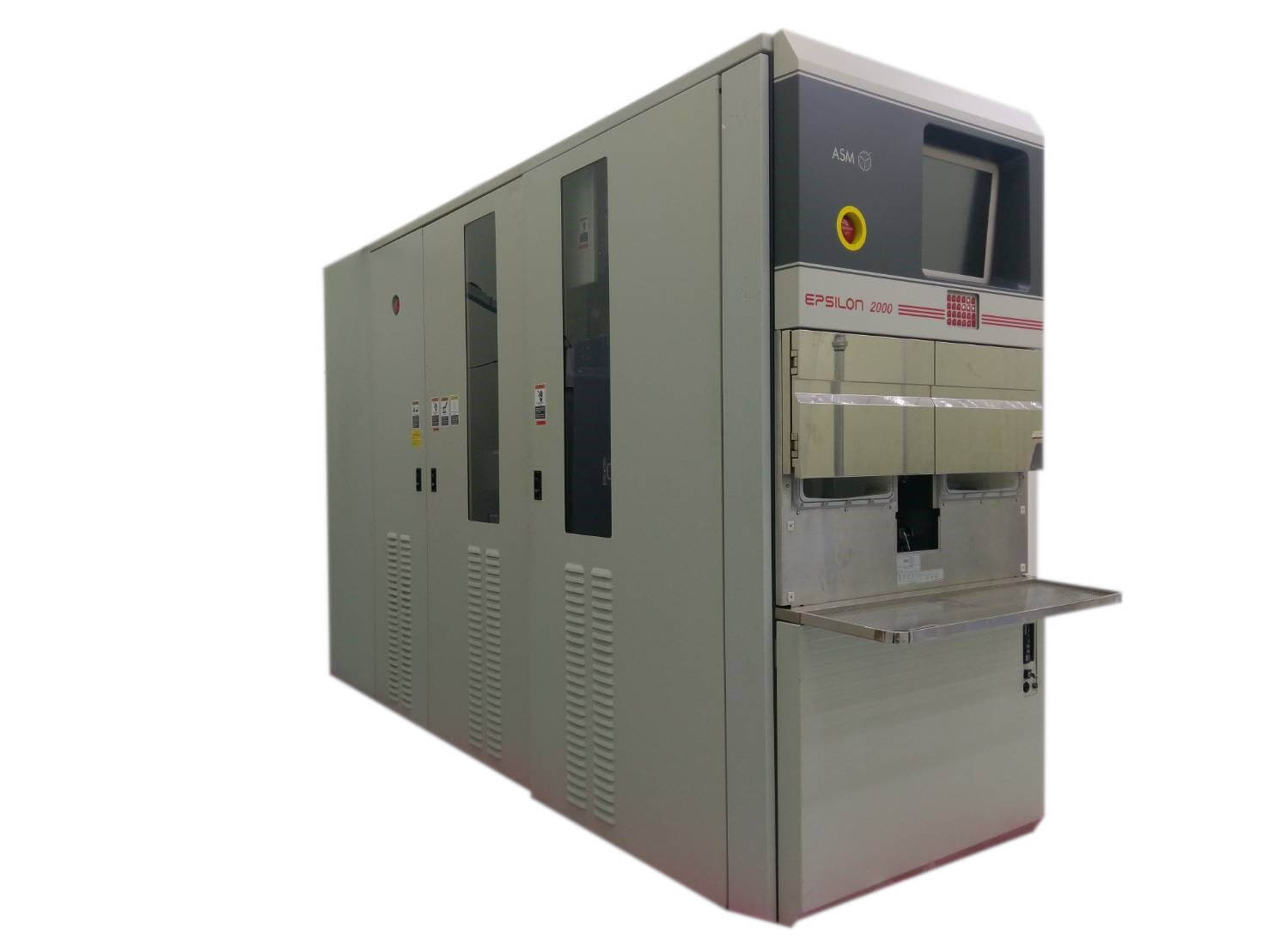
Epitaxy
This process is used to produce thin films of high performance and quality, it can be performed at atmospheric or reduced pressure. Materials grown include silicon (homoepitaxy process), gallium (nitride or arsenide) or even diamonds! Chemical Vapor Deposition (CVD) is regarded as the method of choice for multidirectional epitaxial growth, enabling multiple layer thickness and layer resistance.
It is a versatile fabrication technique, covering a wide range of applications such as Schottky & ultra-fast diodes, power IGBT & DMOS, MOSFET, EEPROM, microprocessors & microcontrollers.
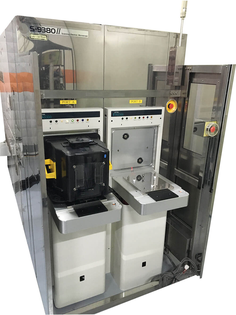
Metrology
Modern semiconductor manufacturing processes include hundreds of steps.
Months of costly labor would have to be thrown away if a defect occurred in the making. To prevent this from happening, metrology logically became the cornerstone of any fab.
Wafers are carefully inspected throughout their production phases to ensure their compliance. The primary objective is to find out which dies are affected by particles or defects on the wafer.
Fully controlling every die would take too much time. Therefore, only a few die per wafer and a few wafers per lot are inspected. If the measurements taken do not fall under a given range, the wafers may be reworked.
Diffusion
Doping diffusion is the method of inserting precisely controlled impurities, called dopant atoms, into the substrate (e.g. a silicon wafer).
This is done to modify its electrical, optical or structural properties. Boron, arsenic or phosphorus dopant atoms are deposed using a solid, liquid or gaseous source (nitrogen, argon…).
To carefully control where the diffusion occurs, a mask is placed onto the wafer, preventing dopant atoms from reaching unwanted areas.
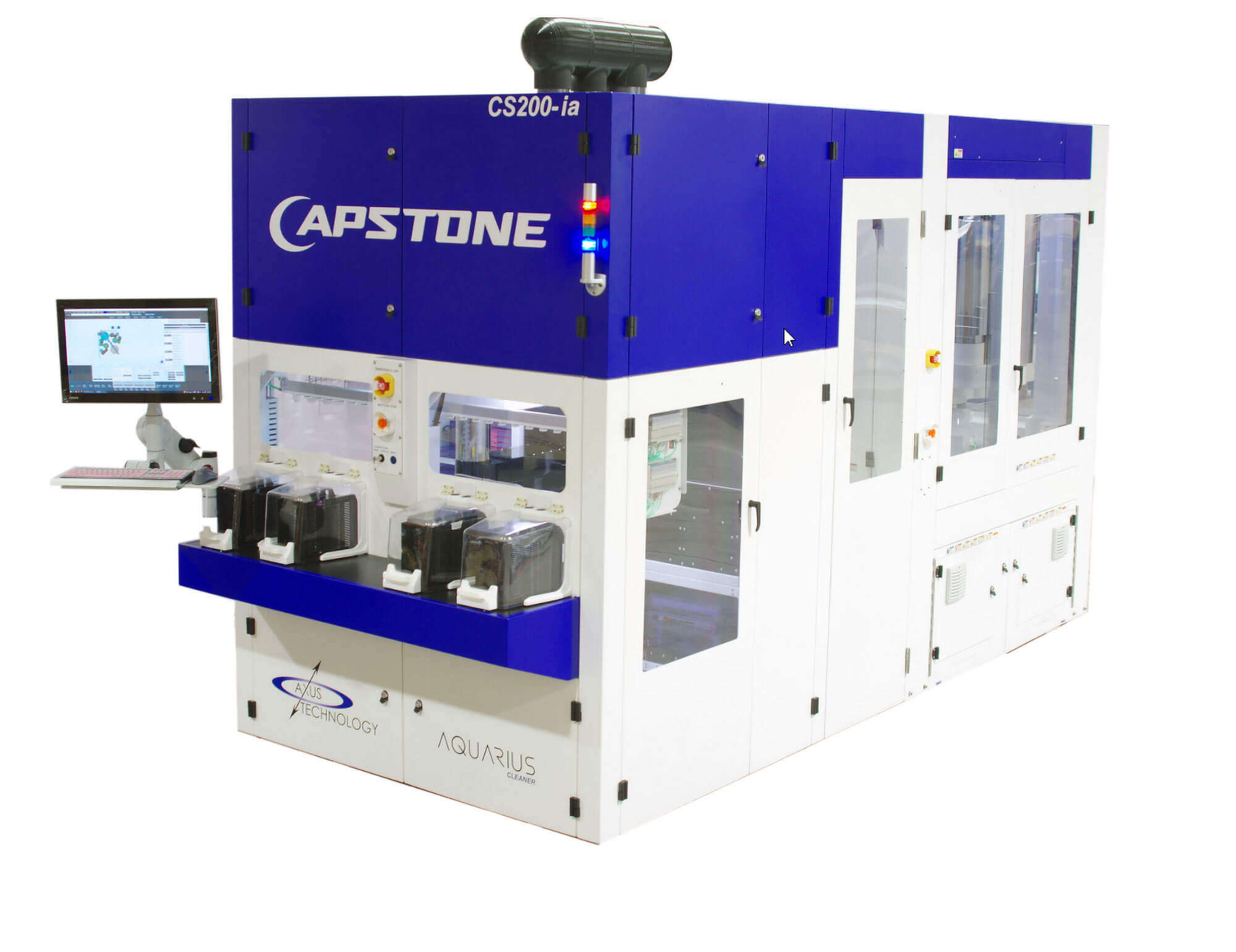
CMP
Chemical mechanical planarization (often called polishing) is a technique used multiple times in the manufacturing process.
It uses the combination of chemical and mechanical actions to uniformly remove material across the wafer. The slurry placed onto the polishing pad is a very thin chemical abrasive. The main objective is to ensure a smooth and leveled surface.
This step can also be taken to correct production defects. Afterward, post-CMP cleaning is necessary as this process induces a high quantity of particles, residues and metallic contaminants.
WET
Wet chemical processes cover a wide range of manufacturing steps such as etching, cleaning and developing.
They are all based on the same principle: a liquid is poured onto a rotating wafer, thus distributing the solution evenly.
Wafer cleaning is meant to remove particles and contaminants from the surface. The coating consists in applying a photoresist onto the wafer surface. A series of photolithography steps are then carried on.
During the development phase, the photoresist is stripped out using organic solvents or acids, leaving the last layer exposed. Wet processes can also be carried out for copper plating.
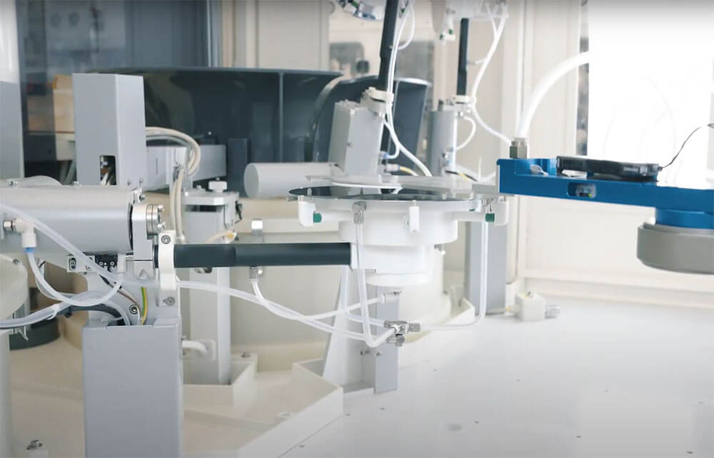
Electroplating
Also known as electrochemical deposition (ECD), the process of electroplating consists in laying down a thin layer of metal onto the substrate.
Wether to increase protection, electrical conductivity, heat resistance or adhesion, this manufacturing step is indispensable to all semiconductors. The plating metal, usually tin, silver, copper, nickel or gold, is positively charged (anode).
The substrate is negatively charged (cathode). Both are immersed in an electrolytic bath. A DC current will then oxidise the plating metal, transferring it onto the wafer, creating an even metal coating.